This article is (hopefully) the first in a series taking a very close look at the “hello, world!” of firmware development: getting an LED to blink on and off.
While we could just copy code somewhere off the web, use a bulking IDE and click a few buttons— which would definitely be the faster way of getting this done— this would not have much of a learning effect. Instead, I want to take the opportunity to go as low level as possible and really understand the mysterious boundary between hardware and software.
I’ll be working on the STM32H573II-DK for this post, which is definitely OP for this task but I just happen to have lying around and for which I have big ambitions.
The hardware setup is suprisingly simple, just plug a USB cable between your laptop and the ST-Link connector and watch it turn on. We’ll skip the messy details of that process for now.
Starting from this point with a few first principles and some basic understanding of how computers work, we should only need a few tools to get this working:
- The code that turns the LED on and off (including startup handlers etc.),
- A toolchain to compile the code for our target device,
- Some kind of CLI tool to flash the device.
After a few simple proompts to Claude with the idea of getting the blinker running with as little tooling and overhead as possible, it gave me back something that seemed like it would work.
Firstly, we need to install the Arm GNU Toolchain (item 2) and also the STMCube_Programmer_CLI, which is part of the STMCubeProgrammer software suite (item 3). I won’t go into the details of putting these correctly onto our $PATH here.
Claude structured the code by providing a main.c file that included the blinking logic, a linker script, and another startup.c file that takes care of some of the MCU intialization.
With mixed feelings of horror and delight, the code compiled, linked and flashed successfully to the device. Although with a great deal of relief that my job hasn’t yet been completed automated, once the device restarted, there was no blinking LED to be seen. Time now for some detective work to figure out what’s happening, and a fantastic opportunity to learn about MCUs.
For the rest of this article, we’ll dive into verifying the blinking logic in main.c and understand what Claude did there line by line. (Perhaps we get lucky and Claude just hallucinated a register address that doesn’t exist.)
In future articles, we’ll take a look at compilation, linking, bootloading and the rest of what’s going on here. Even when we limit ourselves to just the blinking logic, there’s a lot to unpack!
We’re in fact going to make it even simpler for now by just turning the LED on, sidestepping any issues in choosing a frequency that we might notice in a mortal lifetime. So the code for our first “blinker” looks like this:
#define RCC_BASE      0x44020C00
#define GPIOI_BASE    0x42022000

#define RCC_AHB2ENR   (*(volatile unsigned int *)(RCC_BASE + 0x8C))
#define GPIOI_MODER   (*(volatile unsigned int *)(GPIOI_BASE + 0x00))
#define GPIOI_ODR     (*(volatile unsigned int *)(GPIOI_BASE + 0x14))


int main(void) {
    RCC_AHB2ENR |= (1 << 8);

    GPIOI_MODER &= ~(3 << 18);
    GPIOI_MODER |= (1 << 18);

    GPIOI_ODR ^= (1 << 9);
    while(1);
}
One thing to understand off the bat here is the concept of memory-mapped IO (MMIO). I highly recommend this video to get an understanding of what we’re doing here.
Essentially, all of the peripherals (including the GPIO pins that control the LEDs) are mapped onto the same address space that the controller uses for its main memory. So what the code is doing is #defineing the register addresses that we need to set and then in the main function we have the logic of actually setting values at those addresses.
Three other things we’ll need to help us understand this code are the reference manual for the STM32H573xx, RM0481, the datasheet, and the user manual for the development kit, UM3143. We’ll be picking bits and pieces out of these to build up our knowledge of the hardware.
The wheels on the bus…
What’s happening physically on the device when we try and set a GPIO pin to control an LED is that our compiled code causes the CPU to output signals onto a particular bus which connects the CPU to the output pins.
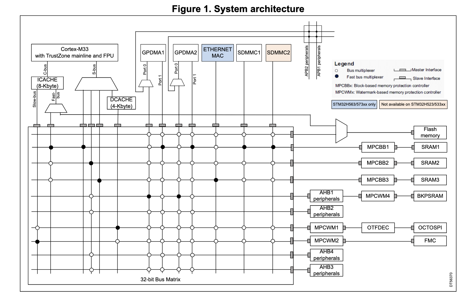
For the STM32H5, the GPIO pins are all connected to what’s known as the AHB (advanced high-performance bus), a protocoll under the umbrella of ARM’s “Advanced Microntroller Bus Architecture” (AMBA). In fact, they are connected to the second AHB, AHB2 (there are a total of 4 of these buses in this chip).
This is where the AHB2 comes from in the register RCC_AHB2ENR.
All of the different buses are connected to the CPU via the “bus matrix”. The architecture diagram in section 2.1 of RM0481 shows us exactly how the AHB2 is connected:
Time is relative
But what about the RCC part? To understand this, we can turn to chapter 11 of RM0481: reset and clock control (RCC!). Essentially, many of the different parts of the system are connected part of their own clock domain. By turning a clock on or off, we can enable or disable that entire part of the hardware.
On the STM32H5, there are a total of 48 different clock regions that we can set. Each of these clocks are themselves controlled by RCC registers, which behave just like all other memory-mapped registers, beginning at the boundary address 0x4402 0C00. This boundary address is exactly the RCC_BASE that Claude set for us in our blinking logic. (This boundary address itself maps to the AHB3—see section 2.3.2, Table 5— suggesting that the RCC registers themselves are peripherals! Note as well that there is no RCC to control AHB3, since presumably it always has to be enabled).
The clock domain we are interested in is the one for AHB2: RCC_AHB2ENR. (The ENR I guess stands for enable register?) at address offset 0x08C (see section 11.8.27 of RM0481). So again, Claude is spot on here.
Within each domain, there are also clock gates, meaning that, although all of the peripherals connected to a particular clock domain will run at the same frequency, we still have fine-grained control over which peripherals are even connected to the clock, allowing us to save power for those peripherals of a particular clock domain not in use.
After a system reset, all of the peripheral clock gates for RCC_AHB2ENR are set to 0. This is why our main loop has to set something to 1 before anything can happen. But why then does it set the 8th bit?
That’s a lot of pins!
Let’s have a closer look at the layout of the RCC_AHB2ENR register from section 11.8.27:
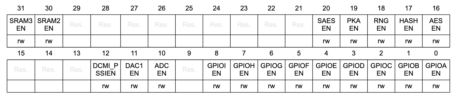
We see 9 different gates for GPIO peripherals, ranging from GPIOCA to GPIOCI.
According to the datasheet, the STM32H573II SoC comes in a variety of packages. Which one we have on the devkit is mentioned in UM3143, the UFBGA176, which has 176 balls or connections, the layout of which we can see in the datasheet:

All of the balls starting with P correspond to GPIO pins. In total, there are 139 of them, organized into different ports. Each port A-H contains 16 pins, and port I only contains 11.
The different gates in our RCC register then correspond to the different GPIO ports. So we can turn on the clock for port B, for example, by setting bit 1 to 1 in RCC_AHB2ENR.
To figure out which port we need for one of the user-controllable LEDs on the devkit, we turn again to the user manual. In section 14.11: Buttons and LEDs, to control User LED1, we see we must set a “low-logic level of 1” to GPIO pin PI9. So looking back at our RCC register, GPIO port I is activated with the 8th bit! So again, Claude got it right.
The general in GPIO
Now we’re almost equipped with all of the background knowledge we need to understand the rest of the logic. Now we just need to understand where the 9 in PI9 comes from and we can close this chapter of the case.
GPIO pins, as their name suggest, can seemingly do quite a lot. They have their own section in RM0481, describing all of the different registers available to configure and control any one of the 9 GPIOx ports.
A GPIO port can be set into roughly 4 different modes: 1) input, 2) output, 3) analog and 4) “alternate function”. For our purposes, we want to put out a signal at some frequency, so we need output. To configure pin 9, we have to set the mode according to section 13.4.1:
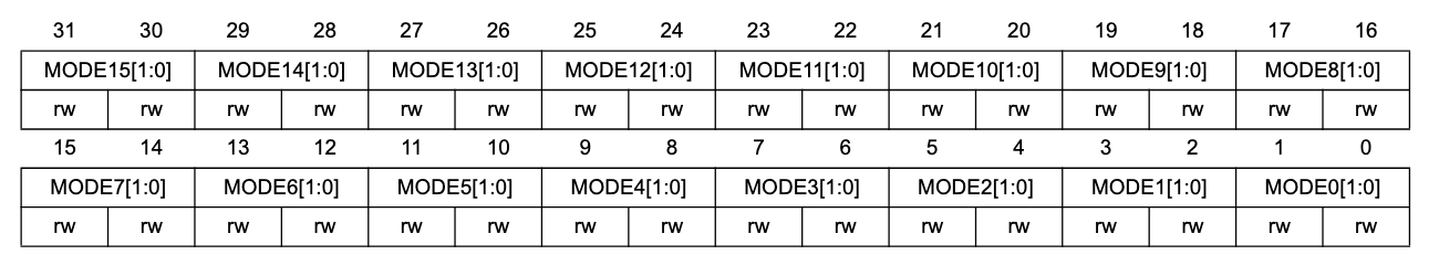
For each pin we have 2 bits to set one of the 4 modes. For pin 9, this then corresponds to bits 18 and 19. For the output mode, we set need to set 01, which Claude does faithfully with:
GPIOI_MODER &= ~(3 << 18);
GPIOI_MODER |= (1 << 18);
And finally, to set the output to 1 as per the devkit user manual, we need to then set the GPIOx_ODR (for output-data register) to 1 at the bit with index 8:
GPIOI_ODR ^= (1 << 9);
So all up, Claude nailed the all the register values. I think we can safely conclude that the issue doesn’t lie in the logic itself. But no fear! We have a few more suspects to interogate. In the next article, we’ll unpack flashing and bootloading, step by step, to see that the code we think is running is actually where it should be.
I hope this post is of some use to someone out there, or perhaps to a future version of myself. My understanding of firmware development so far is that it involves a great deal of cross referencing between all of the different manuals available for our target hardware.
I think it also highlights the value of LLMs as mentors in diving into new areas; as aids to human understanding, not a threat to it. For, after all, as quickly as Claude figured out what code to write, it got it wrong, and it needs us to get to the bottom of it!