The goal of this article is to connect an electric guitar to the STM32H573II-DK, with the aim of learning about analog circuitry, amplifiers and more about analog-digital converters (ADCs). I’ve always enjoyed playing the guitar, but after several years hiatus I need to find a new angle back in. Doing some DSP on musical signals seems like a great way to accidentally learn some music theory along the way. The circuit itself will be a stepping stone into more advanced areas of electronics.
Setup
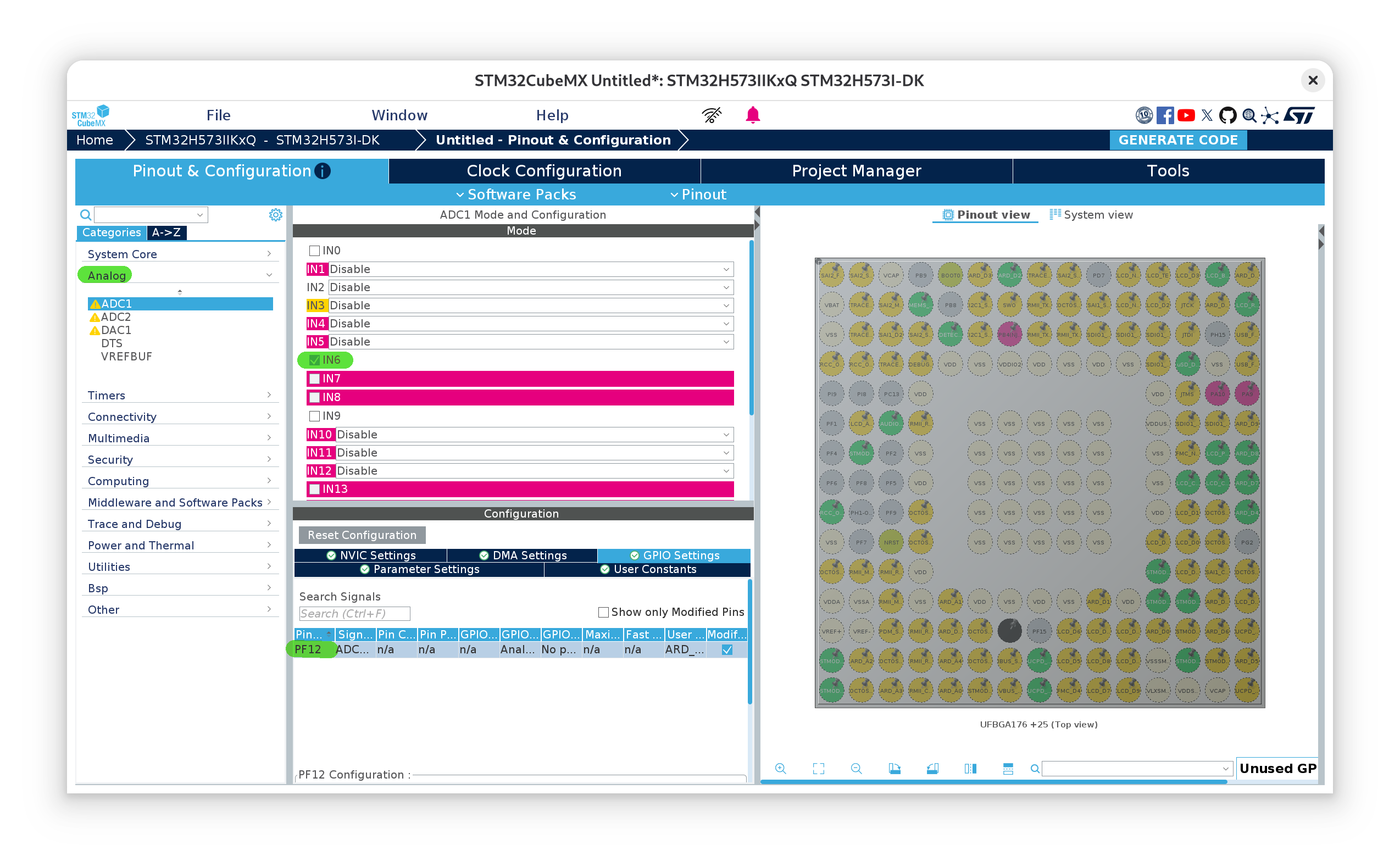
The way the H5 reads and interfaces with the analog world is with an ADC. In a future article, we’ll dive further into its inner-workings and how to use it to its full potential. All we need to understand here is that it can read voltages between ground , (0V) and (3.3V). Each measurement made by the ADC is a 12-bit value (0-4095) spanning that voltage range. The dev-kit user manual, UM3143, table 31, tells us we can find ADC1_IN6 connected to pin A5, which is on the underside of the board in connector CN16 We’ll configure our project using CubeMX to enable the corresponding GPIO pin, PF12 and connect it to the ADC1_IN6:
Be sure to also enable the virtual COM port as we did here so that we can send the values we read back to our host machine.
Our main loop should look something like:
int main(void) {
	HAL_Init();
	SystemClock_Config();
	MX_GPIO_Init();
	MX_ADC1_Init();

	BspCOMInit.BaudRate   = 115200;
	BspCOMInit.WordLength = COM_WORDLENGTH_8B;
	BspCOMInit.StopBits   = COM_STOPBITS_1;
	BspCOMInit.Parity     = COM_PARITY_NONE;
	BspCOMInit.HwFlowCtl  = COM_HWCONTROL_NONE;
	if (BSP_COM_Init(COM1, &BspCOMInit) != BSP_ERROR_NONE) {
		Error_Handler();
	}

	while (1) {
		HAL_ADC_Start(&hadc1);
		HAL_ADC_PollForConversion(&hadc1, 100);
		uint32_t adcValue = HAL_ADC_GetValue(&hadc1);
		printf("%lu\n", adcValue);
	}
}
Notice that reading an ADC value and sending it to the COM port are serial operations. The bottleneck will be the UART connection at 115200bps, which will ultimately limit our sampling rate to about 2000 samples per second. This should be more than enough for measuring the notes on a guitar though.
On the adjacent connector, CN16, we see the GND and 3V3 output pins. We’re going to use the 3.3V power supply from the board itself so that we don’t have to worry about protecting the ADC from extreme voltages.
Finally, we’ll use a small python script to analyse the frequencies that we detect from the ADC. What we’ll do is:
- collect a sample of values from our serial port in a file,
- record how long it takes to collect that sample,
- place the time value at the head of the file and remove any junk produced by our serial-port tool
- then the code will read the time value, use that to calculate the true sampling frequency and generate and display a spectrogram of the sample.
That code looks like this:
import matplotlib
matplotlib.use('TkAgg')
import numpy as np
from scipy.signal import spectrogram
import matplotlib.pyplot as plt
plt.rcParams.update({'font.size': 22})

file_path = '<filename>.txt'
with open(file_path, 'r') as file:
    time = float(file.readline().strip())
    numbers = [float(line.strip()) for line in file if line.strip()]

fs = len(numbers) / time
signal = np.array(numbers)

frequencies, times, Sxx = spectrogram(signal, fs=fs, nperseg=256, noverlap=128)
Sxx_db = 10 * np.log10(Sxx)

plt.figure(figsize=(40, 16))
plt.pcolormesh(times, frequencies, Sxx_db, shading='gouraud', cmap='viridis')
plt.colorbar(label='Intensity (dB)')
plt.title('Spectrogram')
plt.xlabel('Time (s)')
plt.ylabel('Frequency (Hz)')
plt.show()
To collect a sample, then we just have to run the following command
time stm32_log > <filename>.txt
Where stm32_log is my alias for:
alias stm32_log='picocom -f n -y n -b 115200 -d 8 -p 1 --imap lfcrlf /dev/ttyACM0'
Then we play a musical note and stop the collection. For this experiment, I’ll play the high-E string (329.63Hz) 3 times in a row.
Impedance and our first signal
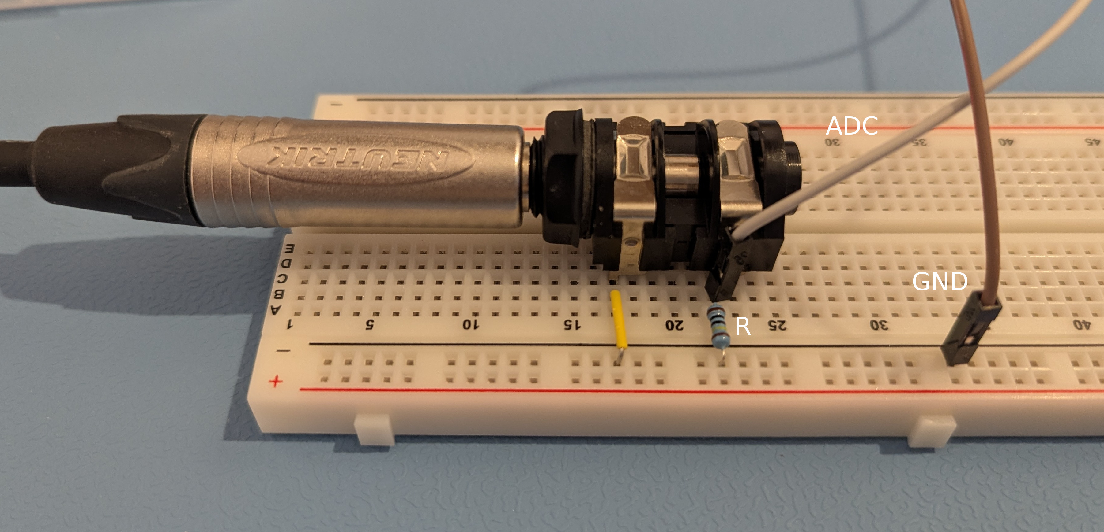
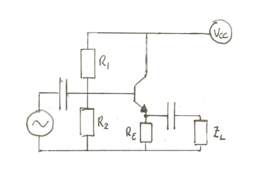
Now, it turns out that a preamplifier is not even necessary to get a reading on the ADC. We can connect the output from a 6.35mm mono jack directly to the input pin. The circuit diagram is pretty straightfoward:
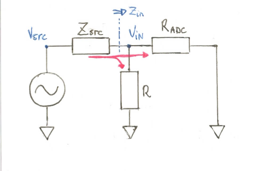
The small-signal analysis of this circuit is simple. There are no DC sources or biasing networks to take into account and the signal is only met with the parallel resistance provided by R and the input impedance to the ADC, as shown by the red arrows.
We can get a sense of the source impedance due to the guitar’s internal circuitry (pickups etc.) by measuring the DC resistance across the tip and sleeve of the 6.35mm plug using a multimeter. For me, this value comes out around 115kΩ, a relatively high impedance. This doesn’t take into account any reactance met by the AC signal, but it does provide us a good lower bound we can start with. In a future article, we’ll try and measure the complete impedance more accurately.
Many similar tutorials on amplifiers use microphones as the source signal. It turns out that microphones have much lower impedances than guitar pickups, which we’ll see, affects our design decisions later on.
For the sake of our calculations we’re going to assume the ADC also has a high input impedance, on the order of 1MΩ. Calculating the exact input impedance for our operating conditions seems like a rather complex endeavour, which we’ll take a closer look at in our future ADC deep dive. However, the H5 reference mentions that the GPIO pins programmed in the anlog configuration have “high” input impedance (section 13.3.12) and measuring the DC resistance between the ADC input pin and GND gave me around 1.7MΩ. We’ll see even 1MΩ dominates any impedance calculations, so it seems like a good value to use.
Treating our circuit then as a voltage divider, the gain at is given by the factor due to the impedance difference in:
To get the highest possible gain, we then need to make sure R is sufficiently high so that A value of 1MΩ gives us a ratio of 0.81. We can measure the RMS voltage of the guitar signal whenever we pluck a string by using the AC-voltage mode. I measured about 20-30mV on average, which means we should expect around 16mV RMS at the ADC’s input. A small value, but it should be detectable.
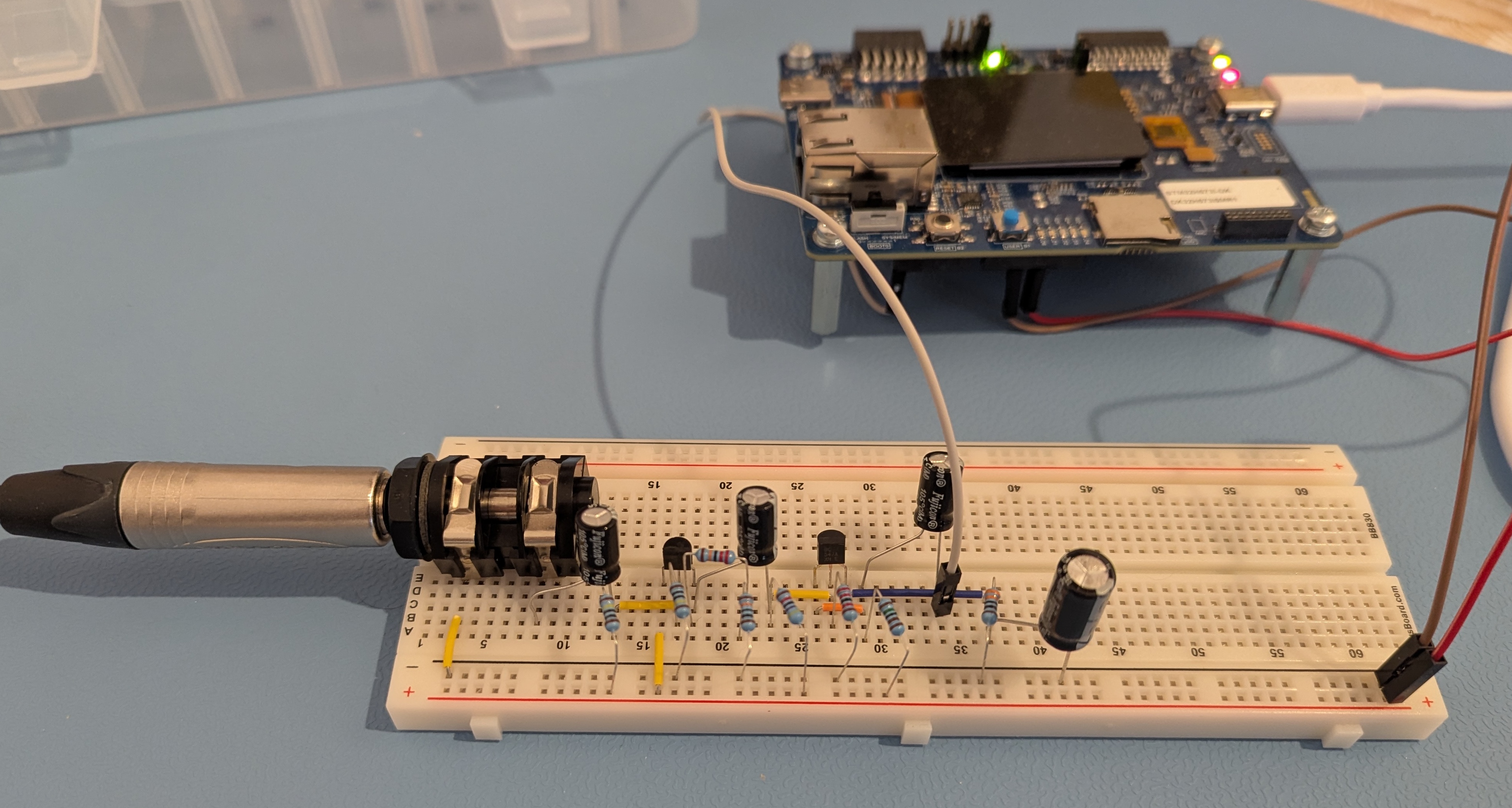
We’ll now run our full experiment, collect a sample, play the high-e string a few times and display the spectrogram as we outlined above:
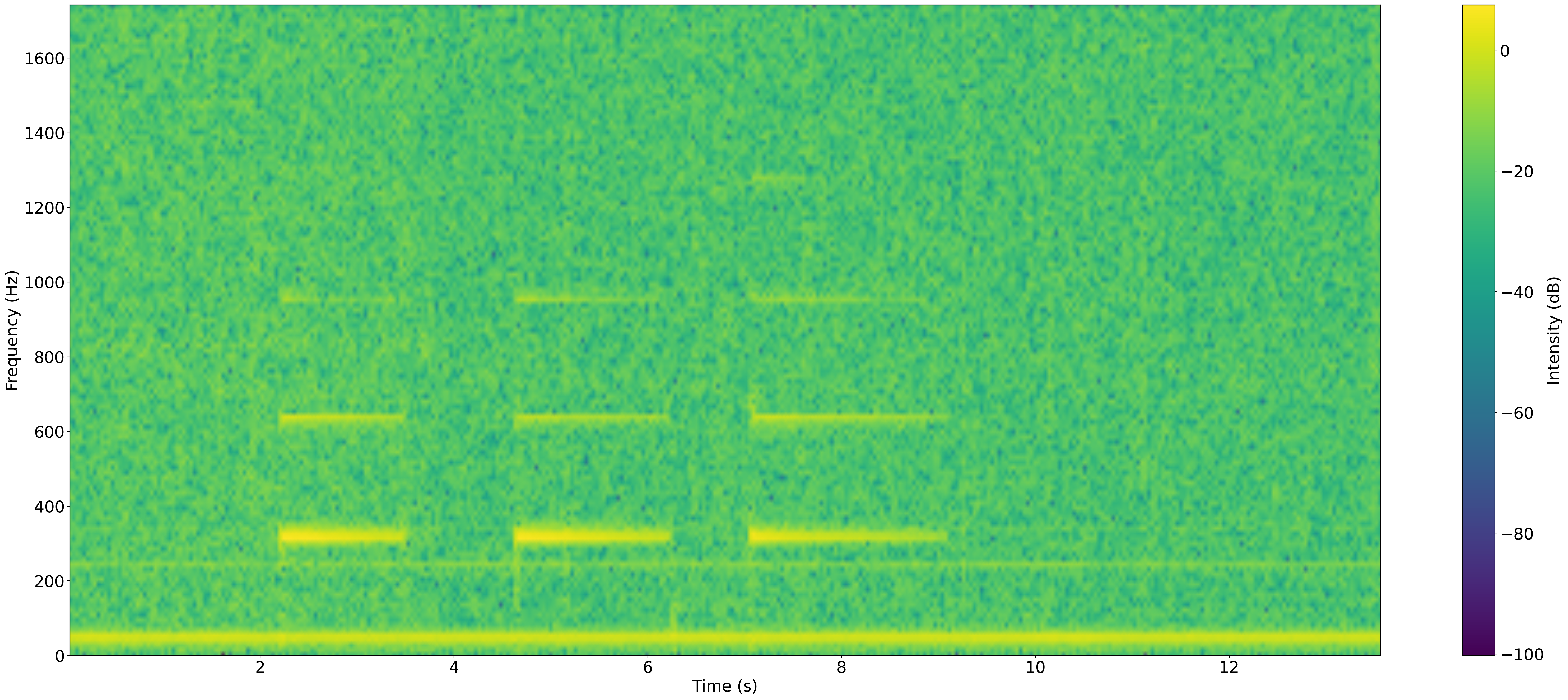
And there we can see 3 neat little pulses around the 320Hz mark! We see the signal strength is not very high, perhaps around 5dB at best, almost as loud as the constant background noise at the 50Hz mark. Supposedly this might be due to the cable picking up EMI interfence from AC mains, and would explain what gives a resting guitar that light characteristic hum.
Notice as well we get the harmonic frequencies at clean multiples of the base frequency. If I remember my high-school physics correctly, these bands should be due to harmonic standing waves present in the vibrating string!
Common-emitter amplifier
The next step is now to see if we can increase the gain on the guitar’s signal so that we can make more use of the ADC’s full range. The simplest we can do is to use a single BJT transistor in a common-emitter topology to provide the voltage gain we need:
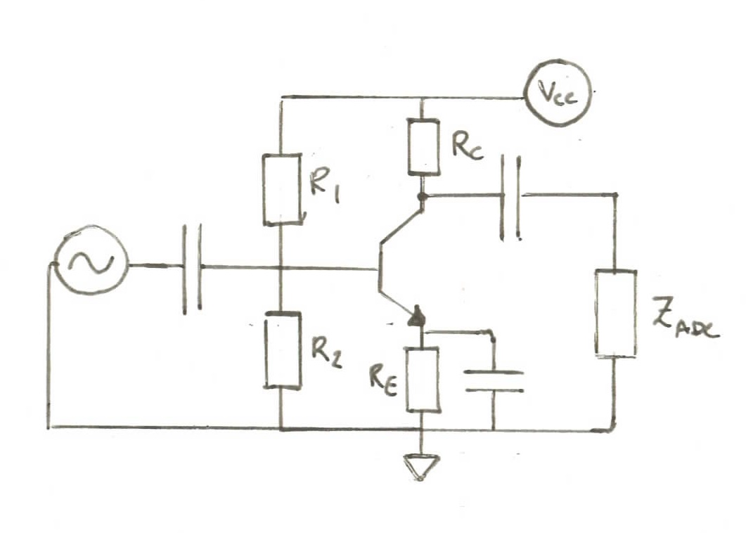
To choose component values, we’ll follow M0NTV’s excellent tutorials on biasing and small-signal analysis and, as per our understanding from our first experiment, aim to create the highest possible input impedance into the circuit so as to avoid as much signal attenuation as possible.
To create the correct bias conditions, we’ll start by aiming for of current flowing through the collector, assuming a β value of 200 for our transistors. We want our output signal to be biased at —i.e. half of the ADC’s input range—for maximum headroom, so we set We’ll take here for convenience. We’ll also pick a of about one-tenth of , or about . This allows us then to calculate .
Finally, we need to now pick resistors for our voltage divider over the base. The base voltage must be to account for the typical diode voltage drop across the base-emitter, maintaining the we set above. We want a “stiff” current flowing throught the voltage divider such that it dominates the current flowing through the base . This ensures the bias voltages we have set are not sensitive to , which can vary quite drastically from transistor to transistor and under different operating conditions. The rule of thumb is that this stiff current should be about 10 times greater than , so for , we’re aiming at . Thus:
.
again, taking and for convenience.
So, now with our biasing values sorted out, we can now derive what the input and output impedances for our common-emitter should be. To do this, we apply the ideas of small-signal analysis.
Starting with the ouptut, we replace the collector-emitter junction with a controlled-current source and remove any (strong-enough) capacitors and DC sources:
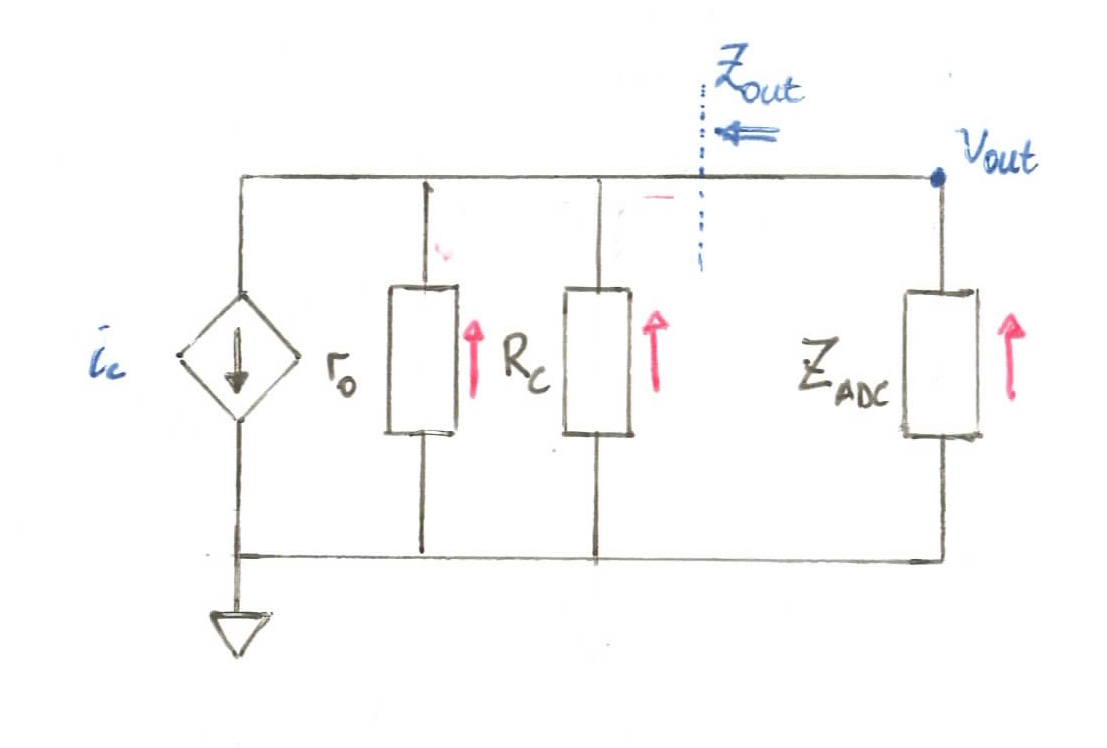
We are assuming that the signal is small enough that the peaks of the signal do not bring the transistor out of the forward-active region. Using the idea of superposition, we then ignore the DC current and only consider the effects of the AC current flowing through the amp. Thus, the current source here is “controlled” by the small fluctions in AC voltage at the base .
where:
We can only do this because in the small-scale model. The 0.7V diode voltage drop has already been taken care of in the biasing circuit, so the AC signal piggy-backs right through the base-emitter junction.
When viewed from the AC-signal’s perspective, current is drawn out from AC-ground through and also from real ground through our load impedance, . The hybrid-pi model we are using here also introduces a resistance as seen by the signal when looking into the collector:
where is the “Early” voltage. Here we’ll use a value of 100V, thus:
However, as this value is so large in comparison to , has very little effect on our output impedance , so we’ll leave it out for the rest of our calculations. In this output circuit, we have a (reverse) current divider, and so we can also write:
substituting our other expression for above, we arrive at an expression for the output voltage in terms of our base voltage, i.e., the gain:
thus:
Plugging in the values we have:
Thanks to the high impedance of the ADC, it has little effect on the strength of the output signal, so this gives us a good idea of the gain provided by our amp!
The input signal to the common-emitter is a bit simpler to deal with. After removing capacitors and DC sources, we see that it faces the following impedances:
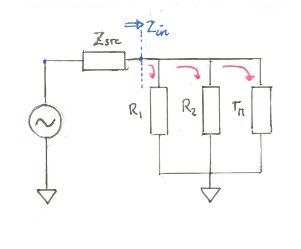
here is the reflected impedance as seen by the signal as it looks into the base of the transistor. Due to the presence of the bypass capacitor after the emitter, the only resistance the signal encounters as it travels from the base to the emitter is the reflected emitter resistance, . Treating our input path like a voltage divider, we can calculate the attenuation from and due to the impedance differences with:
where:
And so we get:
A pretty significant loss! Putting all this together, the total gain for the system is . Roughly a quadroupling in the signal strength. We’ll rerun our experiment now with the amplifier in place. Here’s the spectrogram:
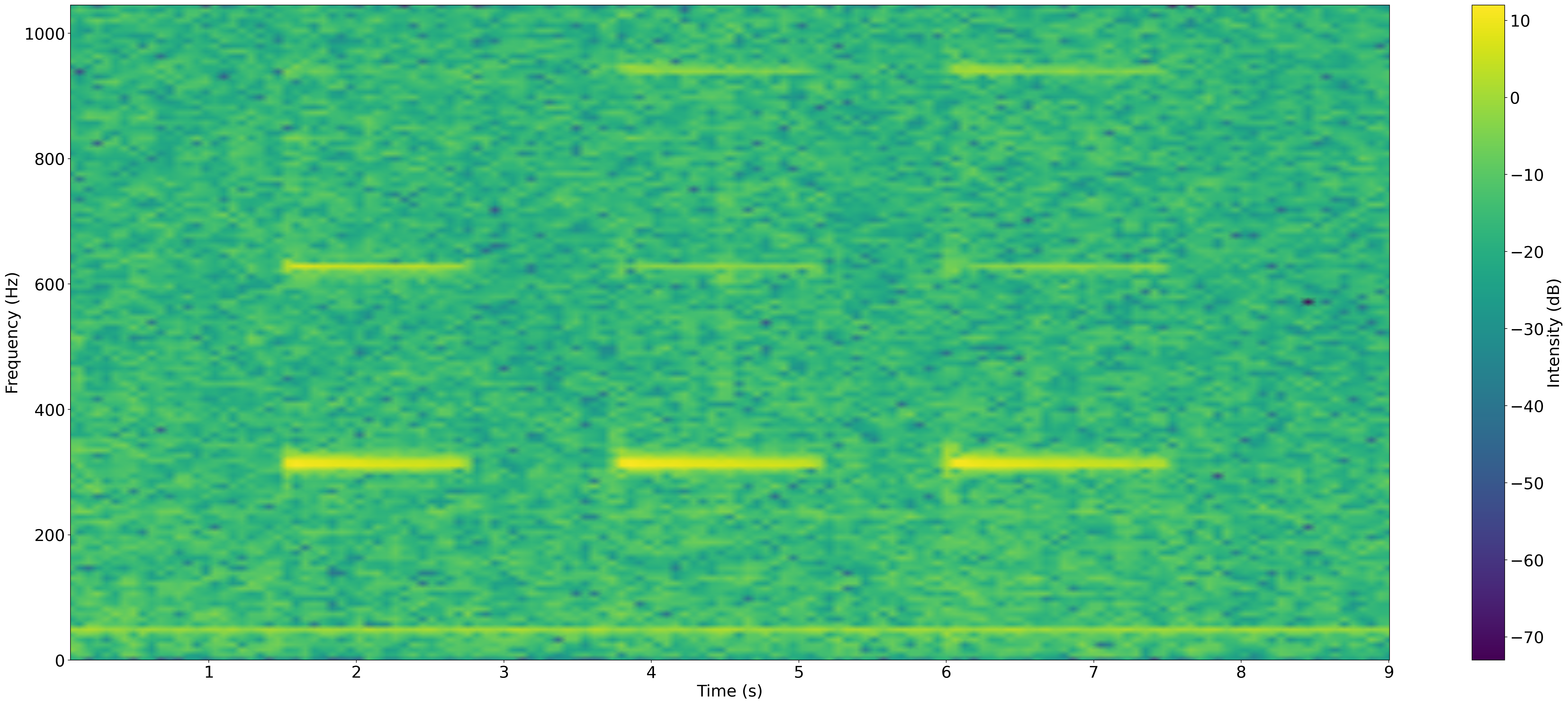
Given that our first experiment yielded signals with about 5dB, now we’re seeing values slightly above 10dB. The difference matches our calculations pretty closely, although due to my inability to play notes with precisely the same intensity, we won’t be able to verify this too accurately. In a future article we’ll look at more precisely measuing the gain. Interestingly, the 50Hz noise has not been amplified quite as intensely as our signal. Perhaps the capacitors in the amplifier are playing a role here? Something else to dive into in a future article!
Emitter-follower buffer
To get higher gain from our amplifier we need to “buffer” it from the high-impedance of our guitar output. We’ll do this using the common-collector, also known as the emitter-follower amplifier. The emitter-follower is known as a unity gain amplifier, as it doesn’t actually provide any gain on the voltage signal. Instead, we’ll use its high input impedance to avoid attenuation at the guitar-signal input. The emitter-follower circuit diagram is as follows:
We’ll start here with the small-signal analysis for our input path, as that will help us decide which reistances to choose for our three resistors:
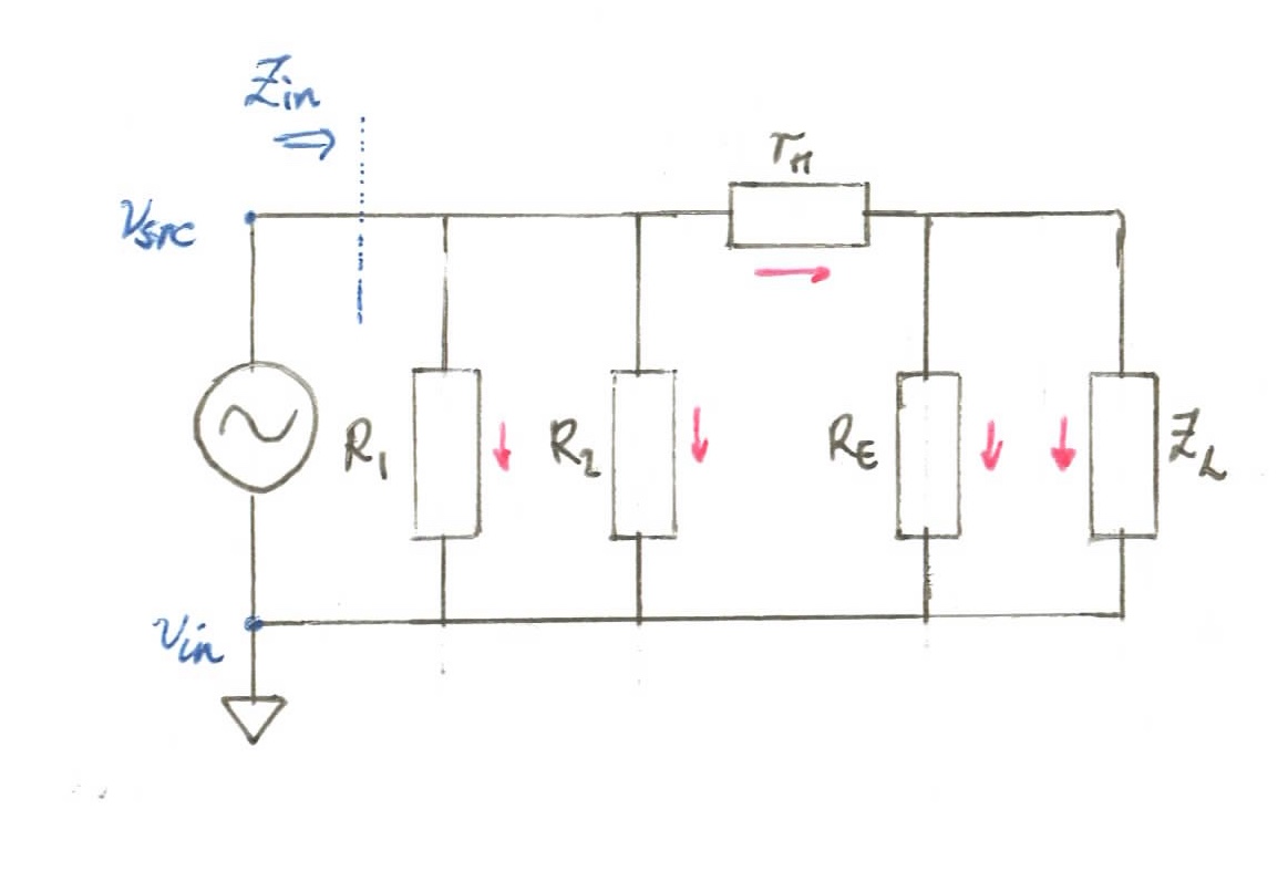
As the signal comes in from the guitar, it’s met with the parallel resistances:
Now, to get this as high as possible, we have three variables: , and . However, similar to above:
and since (the only resistances encountered by the DC current on the collector-emitter path) we then want to choose as small an as possible so that we have maximum resistance. If we settle on , then we get:
And so . Now we see that is now constrained by our choice of , which turns out to be:
We’ll use 330kΩ for simplicity.
To ensure our circuit is properly biased, we only have to ensure that our collector voltage is higher than the base voltage, and that the base voltage is at least 0.7V higher than the emitter voltage, such that the transistor remains in the forward-active region. To get the highest possible collector voltage, we simply tie it directly to our DC power supply with no resistance, such that . To simplify our calculations, we’ll pick a so that .
From our small-signal analysis above, we have the value of the resistance looking into the base of the transistor:
The load impedance is now the input impedance of our collector-emitter circuit from above, 3.75kΩ. Thus the rather large term we calculated above dominates. This means we can pick values for and that make full use of this resistance. If we pick 1MΩ each, then the full input impedance becomes:
And so now we can calculate the attenuation between the source and our buffer:
That’s looking a lot better! Let’s just hope the output attenuation isn’t too bad. So far, I’ve struggled to find a good diagram of the output impedance that makes a lot of sense. Most tutorials I’ve seen gloss over or omit various values for simplicity. Perhaps someone can point me to one. However, we can still imagine the resistance by looking back into the circuit, noticing that the signal encounters parallel resistance from and the resistance looking back up into the transistor. To ge that resistance, we reflect the total resistance seen on the other side of the transistor, , and so divide it by β, and notice that it’s in series with the resistance at the emitter. The equation for calculating the ouput impedance is then given by:
Plugging in our values, we get:
Using our voltage divider rule:
This is looking a lot better than the -30dB that we lost before due to the impedance mismatch. If we replace that with the sum of the attenuation seen due to the input and output of our buffer, we get a total gain for the system of:
Let’s run our final experiment and take a look:

And there we go, we’re seeing signals with powers around 30db, a bit less than we would expect from our calculations, but given the imprecision of the experiment, not too bad! We’ve confirmed we’re getting significant gain thanks to our preamp circuit. Now, there seems to be a fair bit of extra noise here, which would be worth better understanding. Another issue I’ve noticed is that the frequency bins corresponding to the highest signal strength are slightly less (around 310-320Hz) than the value for the high-e string (329Hz). So perhaps there is some interference being caused by the capacitors.
Speaking of the capacitors, I only mentioned them briefly throughout the article, but for musical notes, as long as they’re in the tens to hundreds of μF range, that should be plenty strong enough to allow the musical frequencies to pass through unattenuated.
In future articles, we can take what we’ve built here and go deeper into:
- power amplification, and add a real speaker,
- building a tuning app or chord detector,
- using op-amps as our amplifiers,
- optimizing the gain,
- reducing the noise,
- ADC internals
and much more.
Cheers.