In the last article of the series, Claude gave us the basic logic and build steps for flashing a minimal LED-blinking app, which, thankfully for my ego, didn’t work first go. After doing some detective work and concluding the right registers are being set the right way, we now have to turn our attention to the flashing and boot process.
However, to wrap our heads around exactly what the MCU is doing, in this article I want to survey the terrain and get an understanding for where on the board everything is, and how it all connects together. Of course, a board like the STM32H573II-DK has a lot of features—too many to go into in anything less than a whole text book—so here I’ll focus specifically on the components required to go from power on, to running our code and to turning on the LED, as well as point out a few interesting landmarks on the way.
For our tour on this landscape, we’ll need a few travel companions. We’ll be spelunking down into the depths of the Cortex-M33 processor architecture itself, so we’ll need 3 key documents:
- the Cortex-M33 generic user guide (the GUG),
- the Cortex-M33 technical reference manual (the TRM), and
- the Armv8-M architecture reference manual (the armv8-M RM)
As we’ll as our familiar friends:
- the reference manual for the STM32H573xx RM0481, and
- the devkit user manual, the UM3143.
The hope is that by the end of this article, we’ll have an understanding of the separation of responsibilities between the instruction set architecture, designed by ARM, the SoC, and the (devkit) board, designed by ST-Microelectronics, and just how these components interact with each other.
First off, let’s strip away all of the detail and get a bird’s eye view as we circle in on the parts we care about:
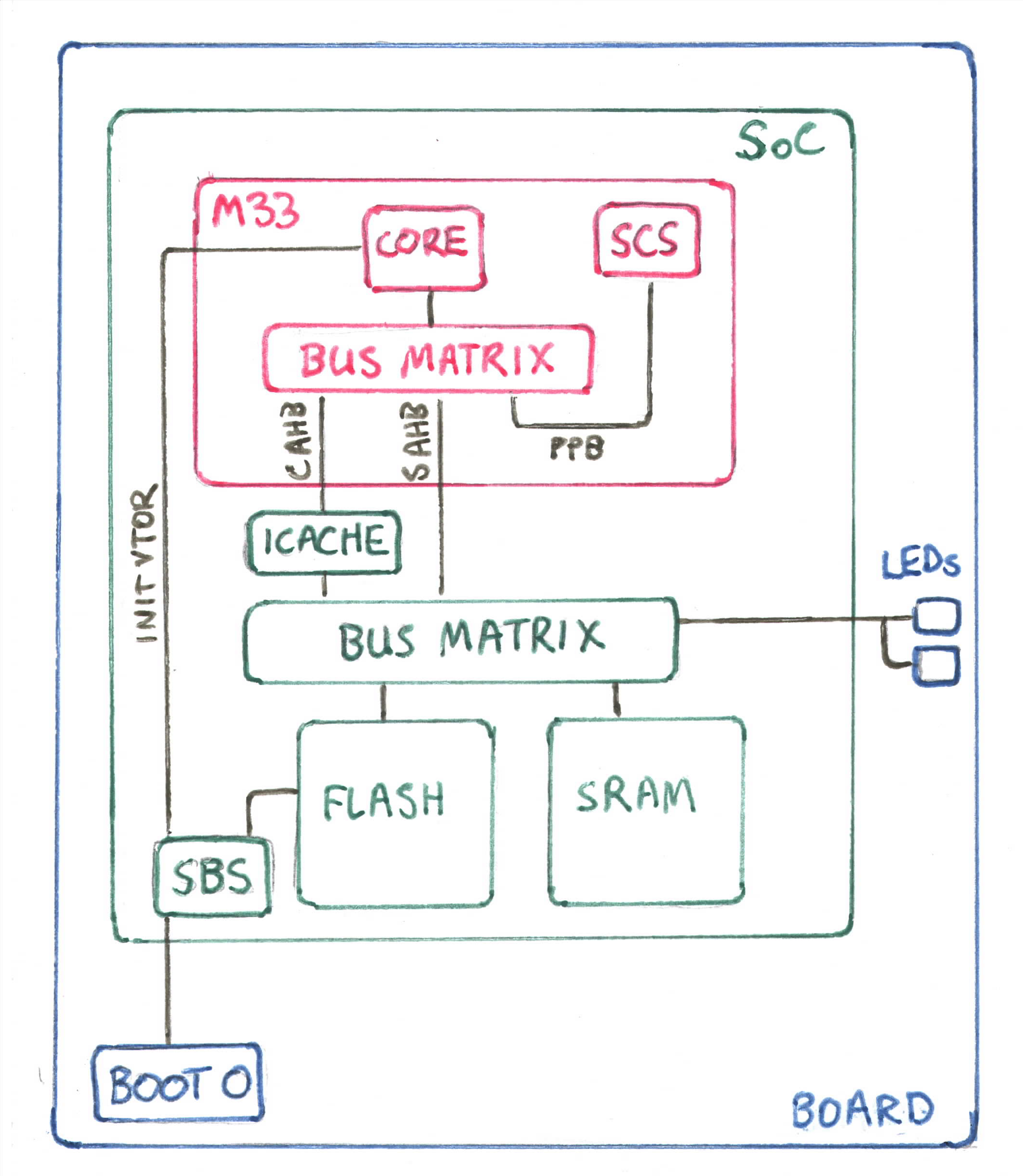
Working from the outside in, we have the development board (blue), which contains a whole bunch of electrical components (connectors, LEDs, an LCD monitor, ICs etc., most of which not displayed here) including the SoC itself.
The SoC (green), as we mentioned in the last article, comes in an integrated package (in the UFBGA176 form), with a series of connections (balls) that are soldered to the dev board. As we discovered, most of these balls are GPIO pins and other forms of IO. Within the SoC, if we were to somehow pry it open, we’d see a similar structure to the board itself: a bunch of little components (the peripherals) all connected to one central component.
And finally at the heart of the SoC is the M33 processor itself (red). As we dive down into the inner workings of the processor, it becomes important to distinguish between the ideal, logical idea of the processor—as we’ll encounter it in the 3 ARM manuals listed above—and the physical implementation of that logical processor that we can hold in our hands, as was put together by ST (or perhaps by some other company on their behalf…).
Where hardware meets software
Our first stop is down inside the M33 processor. There are many components not being displayed here, but the processor itself is divided up into the core and a series of its own peripherals, including things like the FPU, memory protection unit (MPU), debugging modules etc.
We won’t go any deeper physically, (i.e., we won’t concern ourselves with how the core is made up of ALUs, decoders and other basic electrical components) but there is at least one more logical level below the processor layout that is worth understanding: the armv8-M architecture.
In the last article we talked briefly about memory-mapped IO, but it’s interesting to see that the full system memory map is defined at the lowest logical level, in the architecture itself (see the armv8-M RM, section B8.1: the system address map).
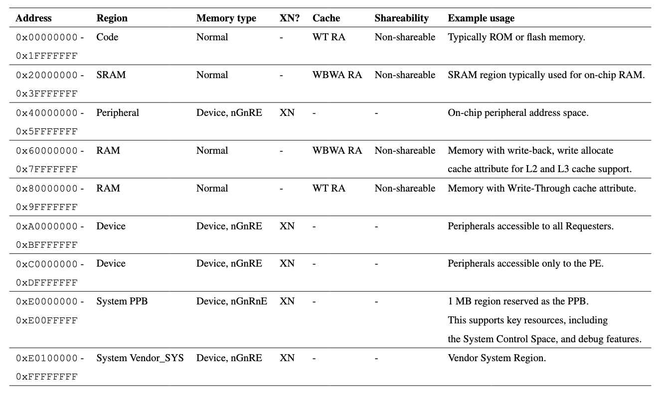
The memory map is thus the logical projection of the physical design choices that have to be made when implementing such a logical architecture. One obvious result of this fact is that a 32-bit architecture can only address 2^32 different registers in memory. But it gets more interesting.
Another more interesting question is: why are MCUs limited to such small amounts of memory? Why don’t they have 4GiB worth of memory, if they’re 32-bit addressable? The memory map already gives us a clue here. The very decision to use MMI/O (as opposed to port-mapped I/O) means that the architecture requires all peripherals to be located on buses that map to the address space. So all of these fancy features that the STM32H5 provides compete for memory within that space. The buses and the interfaces to the processor are of course physical, so the memory map has to reflect these physical limitations.
This highlights an interesting circular causality between hardware and software. It’s wrong to say that the architecture alone constrains the hardware, just as it is to say that implementation of the buses and interfaces alone constrain the software. The architecture was built up over many decades of industry experience in dealing with the behaviour of real physical components, and here the choice of architecture in turn influences just how many interfaces and peripherals can be included in the physical implementation. Kinda cool.
What is a bus, logically?
While we’re down in the pits of the processor, and to further drive home the relationship between software and hardware, I want to examine exactly how the memory map relates to all of the different buses we’ll come across the MCU.
The M33 processor core conforms to a modified Harvard architecture, meaning that there are separate buses for data and instructions. But what does that look like?
In our diagram above, I’ve included the C-AHB and the S-AHB, which stand for Code and System AHB (advanced high-performance bus), respectively. In the section 1.5 of the Arm TRM on interfaces:
The System AHB (S-AHB) interface is used for any instruction fetch and data access to the memory-mapped SRAM, Peripheral, External RAM and External device, or Vendor_SYS regions of the Arm®v8‑M memory map.
and
The Code AHB (C-AHB) interface is used for any instruction fetch and data access to the Code region of the Arm®v8‑M memory map.
The fact that both data and instructions can be fetched from both buses is what makes it a “modified” Harvard architecture, giving us a software-configurable tradeoff between the performance of a strict Harvard architecture and the flexibility of the Von-Neumann architecture.
But how would we tell the processor to use the S-AHB over the C-AHB? Well, we simply just have to make sure our code is copied to a region of the memory map that is serviced by the S-AHB!
This might seem obvious, but for me a light bulb went off as I realized that the memory map IS how you choose what hardware to activate on the MCU, including all caches, memory, I/O channels; everything! This will come in handy as we want to optimize our code in future work, as ST demonstrates here.
Another powerful way of thinking about it is that the region of the memory map that corresponds to a bus is essentially the logical counterpart of the bus itself!
Private peripherals
With that under our belt, we have one more landmark on our tour before we go up for air: the private peripheral bus (PPB) and one subspace of it (that term should make sense now!) in particular: the system control block (SCB) (see the GUG, section 4.2). The SCB contains registers that control many aspects of how the processor operates, all located within the address range 0xE000ED00-0xE000ED8F. (According to the TRM, section 2.4, table 2-1, this means that the registers in this region are physically located within the processor, and don’t go out to the “external” PPB, although these registers are not displayed anywhere, as far as I can tell).
One register in this space that’s worth our attention is the vector-table offset register (VTOR). This register holds the location of the vector table, a contiguous block of memory that contains in its first position the location of where the main-stack pointer (MSP) should be (and thus defining where the stack will live in our address space) and in its second position, the address of the reset handler. (Vector table sound fancy, but it’s really just an array of pointers, i.e., it is itself a vector, not that the elements within it are somehow vectors).
I won’t get into the details of interrupt handling here, as, according to section 2.1.4 of the GUG, the reset handler is the one handler that is executed in Thread mode, so it is neither really an exception (since it’s arguably part of normal operation) nor an interrupt (since nothing was running before it’s entered). But it’ still worth knowing that the vector table is where our exception handlers are registered with the processor.
Threading the needle
With all of that now clear as mud, our journey takes us up again to the SoC level.
As we’ve already tried flashing code to the H5, we might have noticed that we had to flash our code to region 0x08000000. This is where ST decided to address (some part of) their available flash memory. This coincidentally shows how the implementers of the processor and SoC are then free to further chop up the address ranges as defined by the architecture:
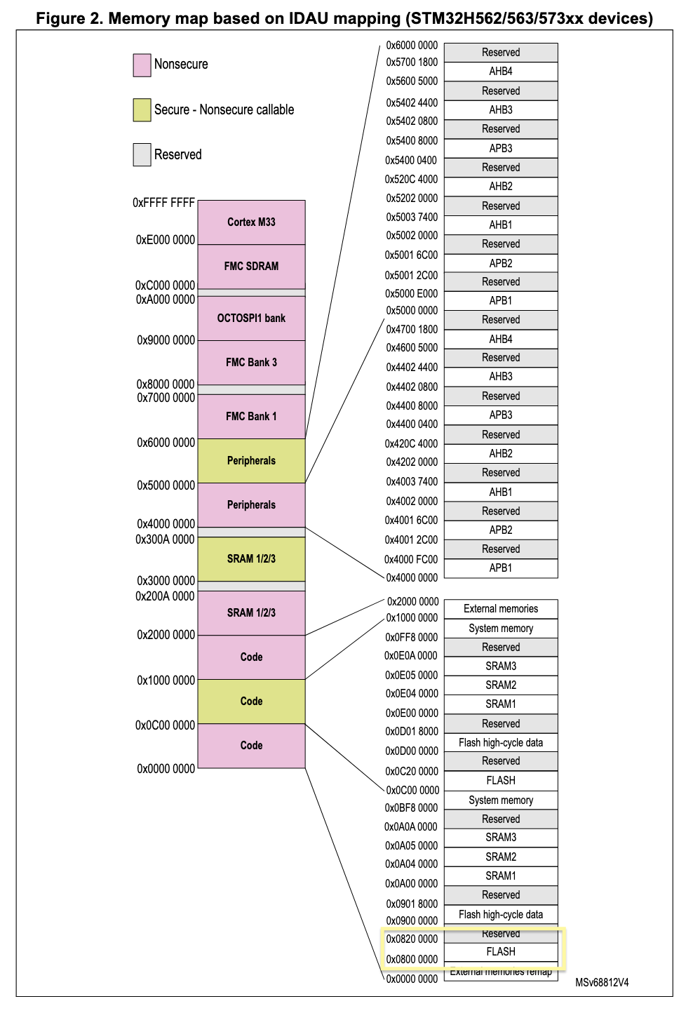
(Compare this with the memory map from the armv8-M RM from above and notice that those address boundaries are still there. For example, all of the Code regions still have to fit in [0x0, 0x20000000))
But wait, the VTOR’s reset value is UNKNOWN (GUG section 4.2.1, table 4-2) so how could our code, flashed to 0x08000000, ever possibly get picked up by the processor?
Well, it turns out that there is a particular peripheral in the SoC, the so-called “system configuration, boot and security” module (SBS, not to be confused with the SCB or SCS in the M33 processor 😱), which modifies how the SoC behaves during boot (duh!).
The docs unfortunately don’t enlighten us too much on how this works, but in table 128 of section 14.3.2 of the RM0481, we see the inputs to the SBS contain, among other things, the BOOT0 pin and as an output, the module provides a signal called sbs_init_vtor. As far as I could glean, and probably glossing over a lot of detail here, the SBS then, on reset, raises the signal value to 0x08000000, causing the processor to use this value for the VTOR (see table 25, section 4.2 of RM0481).
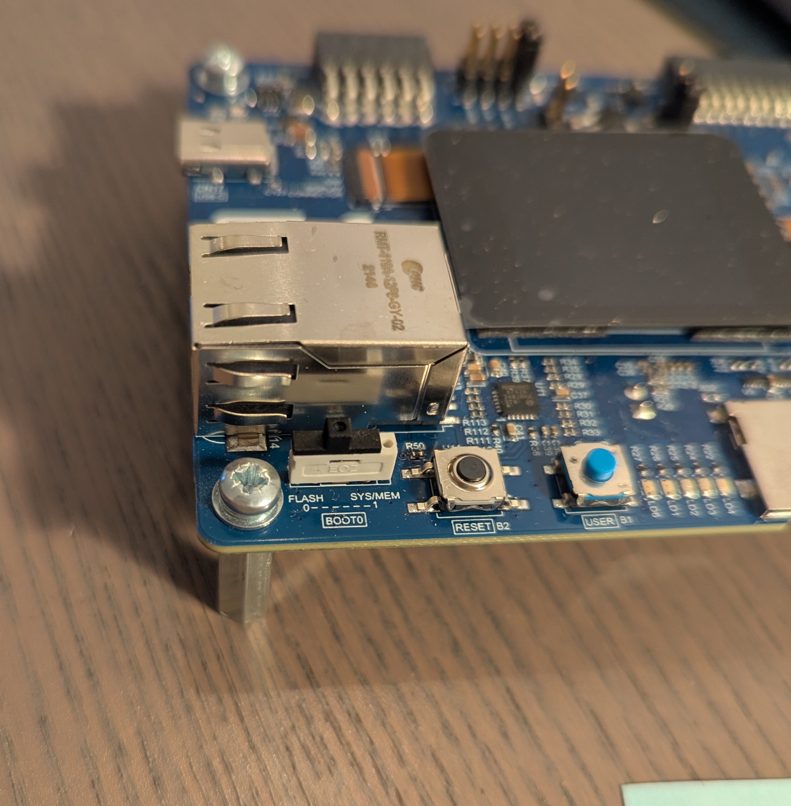
And what’s BOOT0? Well, it’s just a physical switch on the device that we can flick with our finger that routes directly through to the SBS:
And that’s it! Now we’re back up where we started, at the board level, hopefully a bit more knowledgeable about how all these pieces fit together. Ignoring a lot of detail, we saw how (in reverse order):
- the BOOT0 pin’s output signals to the SBS to output the
sbs_init_vtorsignal with a value of 0x0800000, - the
sbs_init_vtorin turn gets picked up by the processor, which sets theVTORregister on the PPB, - the processor reads the location pointed to by
VTORfrom the flash region to find the reset handler, - the reset handler is executed in privileged Thread mode,
and off we go!
We also saw how the memory map is the logical representation of how the hardware is organized and how we would use the memory map to activate any part of the hardware we wanted. In the next article of the series, we’ll use this knowledge to finally understand the boot process from the programmer’s view of the MCU and get our hands dirty with bit of assembly to understand the processor’s internals just a little better, in the hope to finally get this dammned LED turned on!